Using the STM32F030F4 TSSOP20 microcontroller
When this page was written there were only two DIP/DIL ARM Cortex microcontrollers on the market:
the LPC810 and the LPC1114FN28 from NXP. The first of these is easy to get but only has 8 pins so
it has very limited I/O capability. The LPC1114FN28 on the other hand has 28 pins and in theory is
ideal however there is one problem: they are not readily available in Europe and must be shipped from
the USA making them uneconomical if you want to buy just one or two chips. Surface mount chips are
readily available on the other hand and, with a little soldering and a relatively cheap adapter you can
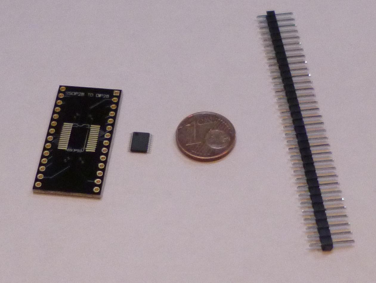
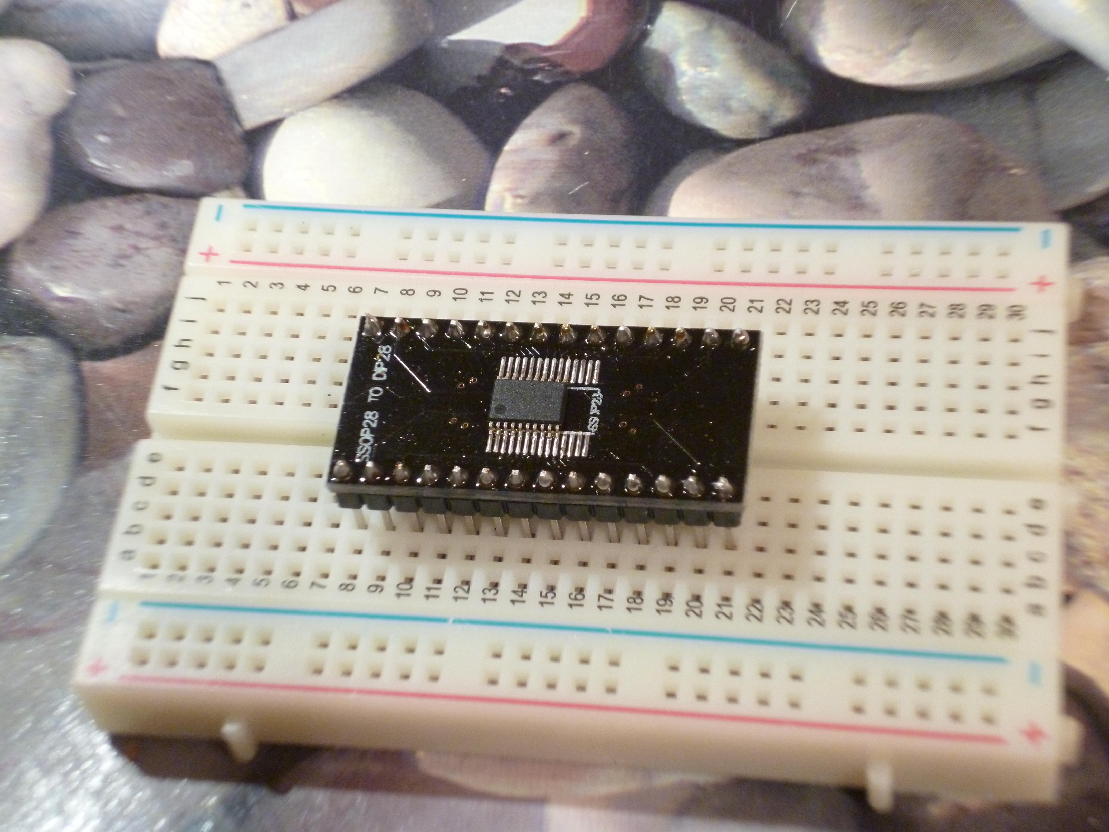
convert these to DIP devices. Figure 1 shows the parts used in this exercise:
An STM32F030F4P6TR which cost 91 cents (plus tax) from Farnell/Element
An SSOP28 to DIP28 adapter which cost 3.52 Euro for a pack of 3 from dx.com
A 0.1" pin header stip which cost 2 Euro for a pack of 20 from dx.com
Skip down to the code
The soldering process
Step 1: Cover the pads you intend soldering with flux
Step 2: Apply solder to the pads in question. Don't worry, the flux and surface tension will make the solder stick to the pads
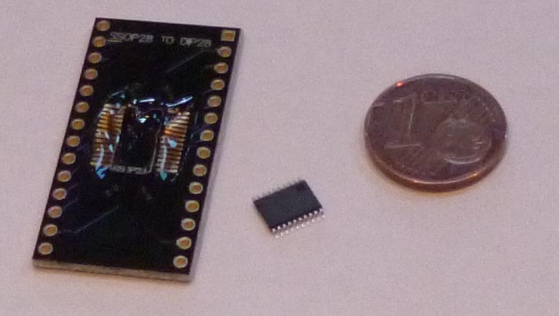
Step 3: Place the chip on the adapter, carefully lining it up with the pads.
Step 4: Carefully solder one of the corner pins in place. You should not need to add any more solder, the coating
you put down in step 2 should be enough. When the joint has cooled, check to see that all
of the pins are still lined up with the pads. If not, reheat the joint and reposition the chip. When you are happy with the
alignment, solder the remaining pins in.
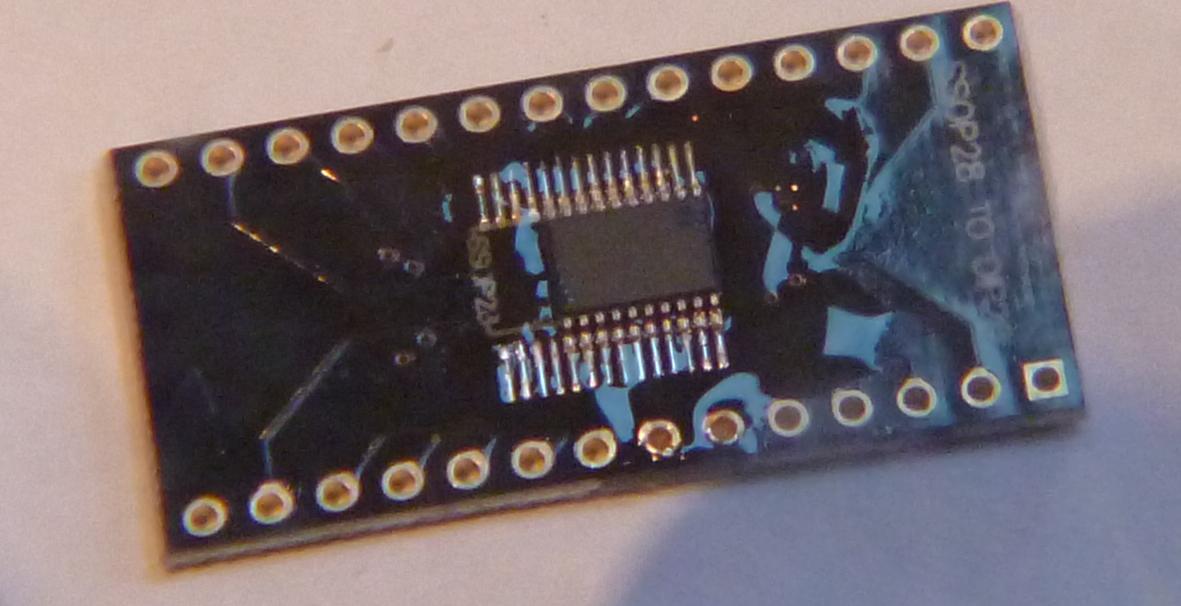
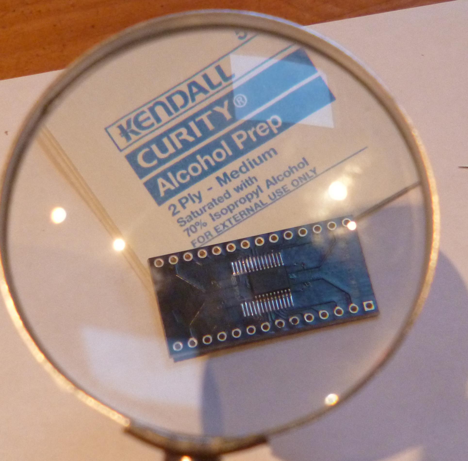
Step 5: Remove excess flux using iso-propyl wipes.
Step 6: Attach the pin headers. I like to use a breadboard to make sure the headers are all lined up properly. As before,
solder one pin on each header, check alighnment and solder the rest in.
ISP hardware setup
The STM32F family of devices support in-system programming. This means that you can program the devices using a simple USB to
serial converter. These converters can be bought online for approximately 2 euro. The schematic diagram for ISP programming is
as shown below.
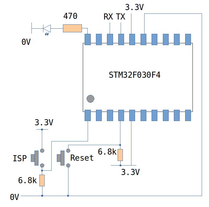
Two buttons are used; one to reset the chip, the other to place the chip in ISP mode. The procedure for ISP programming
is as follows:
Press Reset and ISP buttons.
Release Reset followed by ISP
The chip will now wait for you do download a program using the smt32flash utility.
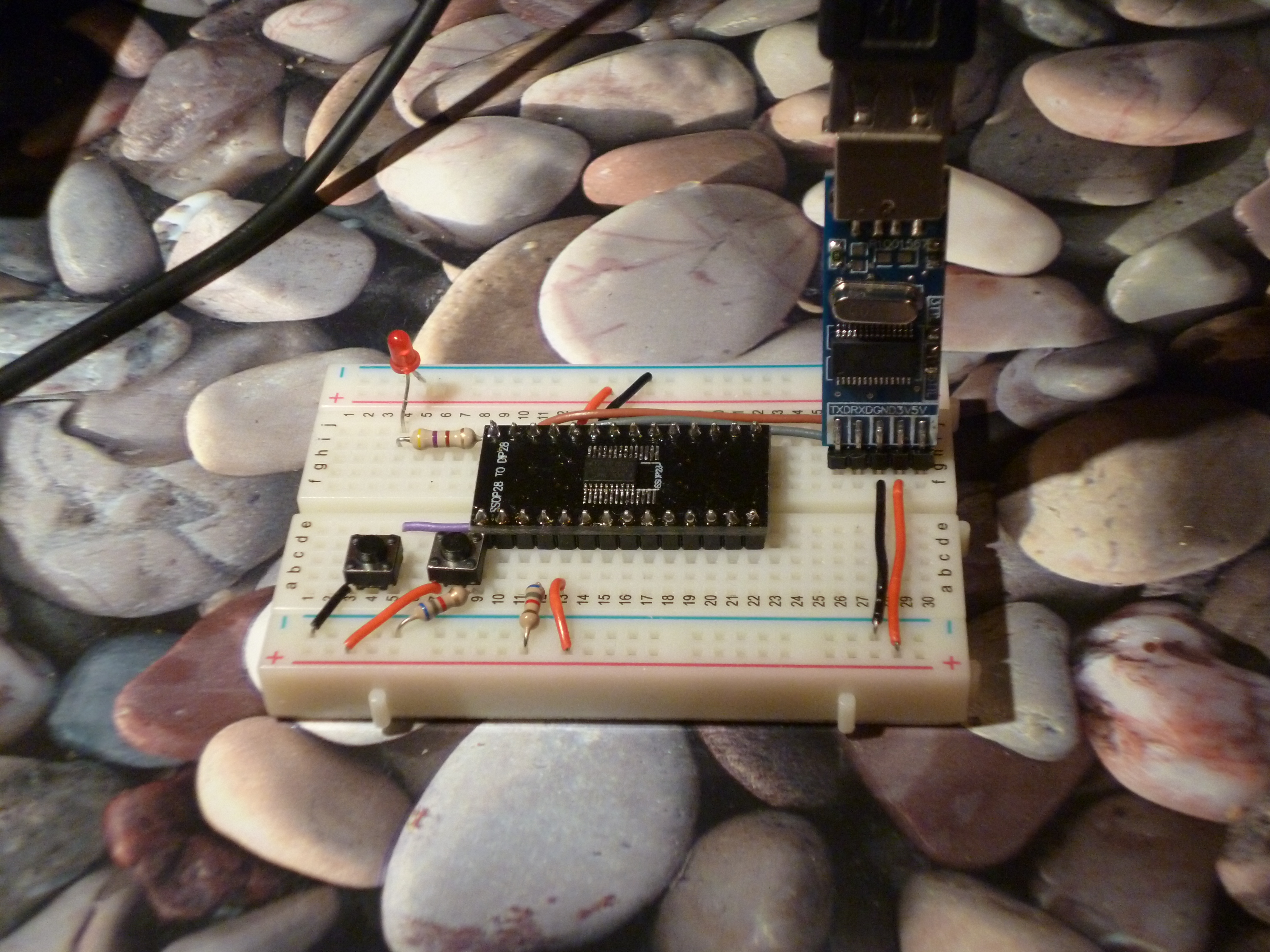
A picture of the actual layout I used is below:
First program: Blinky
The first test program for this circuit is "Blinky" of course: A simple program that flashes the LED.
        int main()
        {
            initClock();
            configPins();
            GPIOA_MODER = BIT28; // make bits 14 an output
            while(1)
            {
                GPIOA_ODR |= BIT14;
                delay(100000);
                GPIOA_ODR &= ~BIT14;
                delay(100000);
            }
            return 0;
        }
The initClock function sets the system clock running at 48MHz. The configPins function turns on GPIO Port A.
GPIOA bit 14 is configured to be a digital output. The program then enters a never ending while loop that sets and clears bit 14
of GPIOA with a little delay between each change. Full source code is available here.
To compile the code you will need GNU make and an ARM GCC cross compiler. You can download the cross compiler
here. If you are running a Linux system you probably already have
GNU make installed. If you are on Windows, go and get mingw and its msys components.
To compile, type make. Hopefully the program will compiler and create a file called main.hex.
Programming the device
The stm32flash utility is used to program the chip. It can be downloaded from
here, You also need a USB serial to parallel converter (and supporting drivers).
I use a device with a Prolific chipset which is supported by Fedora, Ubuntu and many other versions of Linux. When the device is
plugged in it appears as /dev/ttyUSB0. On a Windows machine this might appear as COM3 or similar.
The USB/Serial converter is also used to power the circuit so, assuming wiring is ok, plug it in (and check for stuff getting hot!).
Put the device into ISP programming mode as described above (RESET+ISP, release RESET then ISP) and type the following:
stm32flash -w main.hex /dev/ttyUSB0.
This should program the chip. Hit RESET and the LED should blink.
Serial communications and the ADC
This example reads the Analog to Digital converter repeatedly and prints the hexadecimal value of the conversion results
to the serial port (the same port as used by the ISP programmer). Code is here SerialADC.tar.gz.
Check back for more examples later or look at other development relating to ARM micronctrollers on this site here
Making a low cost wireless sensor node
Given its low cost and integrated ADC, the STM32F030 makes an excellent low cost sensor node. My experiences with it in this role are are documented
here.
The following code uses timer 14 to periodically wake the STM32F030. The chip takes an ADC reading (AN0) and sends it to a node.js script on an Intel
Galileo once every 5 seconds. C-code and javascipt are included in the file. The current consumption drops to less than 0.6mA when sleeping - which is most of the time.
Download the code
Using the RTC Alarm interrupt
The following code uses the built-in RTC and LSI oscillator to wake the CPU from a deep sleep once every second (approx)
Download the code
Using an NRF24L01+ module with the RTC Alarm to produce a very low power sensor node. (Average current consumption around 80 microamps)
Back to home Baremetal ARM page